Equipment
Electron Beam Lithography (EBL) System
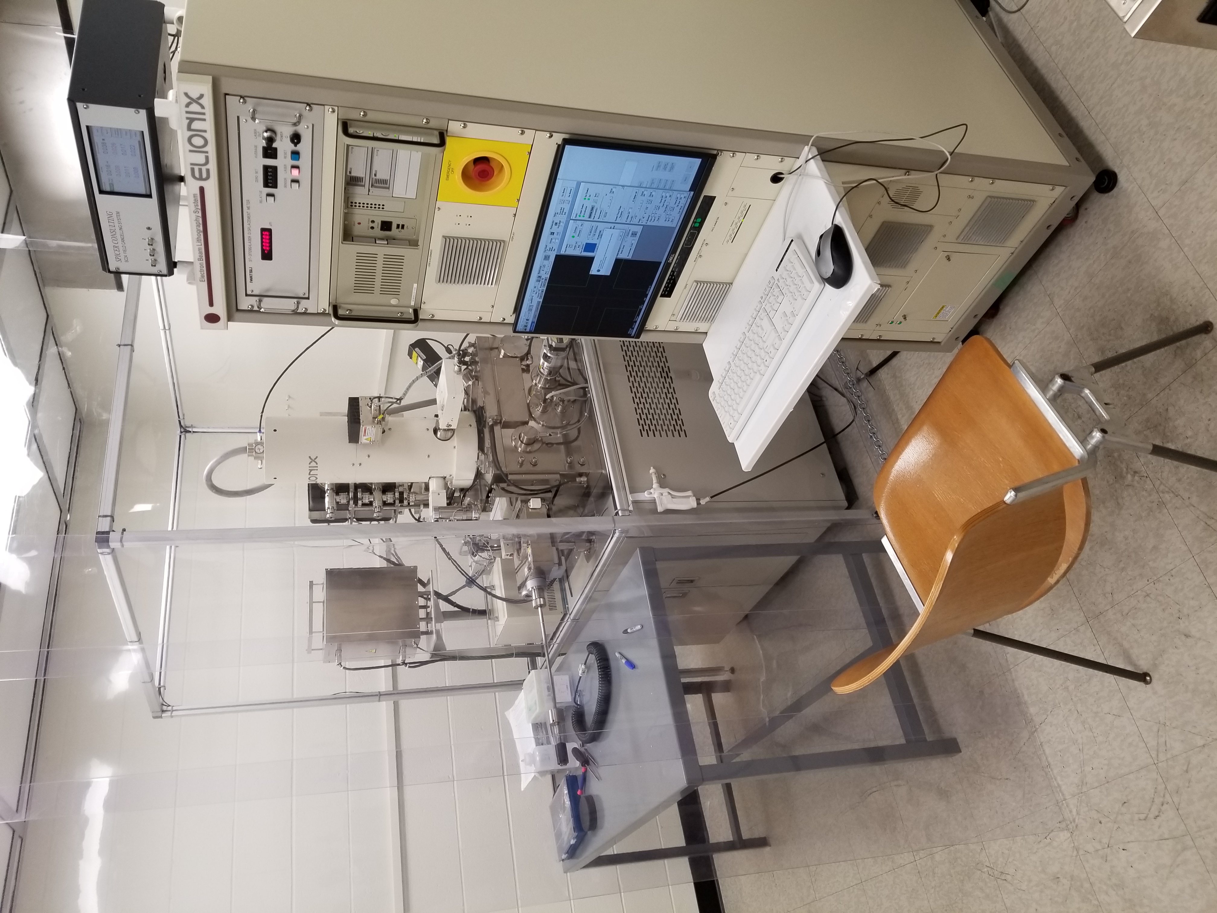
Model:
Elionix ELS-S50EX
Capabilities:
This tool is a high resolution 50kV field emission microscope and lithographic tool using electrons. It is capable of writing features as small as 10 nm over a large field size (3 x 3 mm). It features low distortion beam deflection and high uniformity over the exposure field, and high stitching accuracy (± 20 nm).
Cost:
Calendar for Reservations:
Specifications:
- ZrO/W thermal field emitter.
- 50kV accelerating voltage, 2 nm beam diameter, 10 pA to 50 nA beam current.
- 10 nm minimum feature width.
- Up to 3 x 3 mm lithographic field size.
- Beam positioning resolution: 0.1 nm at 100 μm field, 1.0 nm at 1 mm field
- Field stitching accuracy: ± 20 nm
- Can accommodate up to 6" wafers.
On-line Manual:
Dedicated EBL systems are essentially highly specialized SEMs using electrons for both imaging and high resolution lithographic patterning. With respect to SEMs, EBL systems have improved speed and accuracy (decreased stage positioning error) in order to reliably pattern small features over large areas.