Overview
The clean fabrication area in Goergen Hall is comprised of 2000 square feet of class 1000 cleanroom and a few hundred square feet of support area. An outside gas supply area is included in the design, saving interior space.
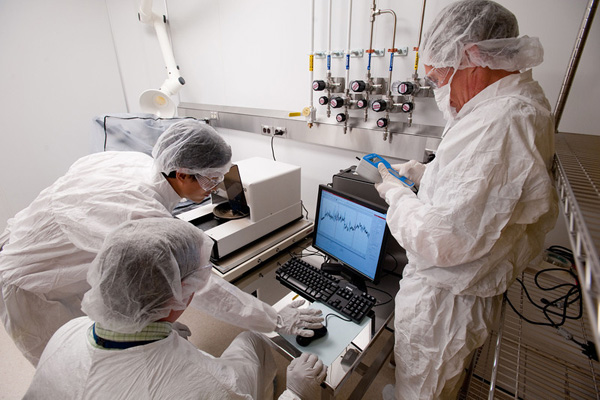
The metrology area for URnano is on the second floor of the Wilmot building and contains about 500 square feet of electron microscope space and about 400 square feet of preparation and measurement space.
It includes systems for:
- Optical microscopy
- Scanning electron microscopy (SEM)
- Focused ion beam microscopy (FIB)
- Transmission electron microscopy (TEM)
- Scanning probe microscopy
Imaging techniques available include:
- Secondary electron
- Back scattered electron
- Scanning-transmitted electron
- Xray emission
- STEM (SEM-FIB has in-situ Pt metal deposition capability)
Also included in this area is a full sample preparation suite including tools for sputtering and evaporation, plasma cleaning, hypercritical drying, microtomy, grinding/polishing and wire sawing. Most samples can be prepared here for high resolution imaging.
Specialized Tooling
The total space occupied by the Integrated Nanosystems Center is divided into three distinct categories, each with its own specialized tooling.
By combining these three areas of concern under one umbrella, URnano researchers are able to start with a design idea and fabricate prototypes and working models of devices and structures, and measure their progress. See the equipment page for a complete list of equipment for each space.
Deposition and Etch
We have the capability to prepare surfaces for nanofabrication through cleaning and selective etching, including plasma processing and CVD activation. This area also provides stations for metal and oxide layering, using evaporation and sputtering techniques, atomic layer deposition, as well as a variety of wet processing areas.
Lithography
This is divided between a photolithographic area in the cleanroom and electron and ion beam processing in the metrology area. The former contains a manual exposure tool for up to six inch substrates and associated bench processing; the latter, beam writing interfaces to state-of-the-art electron and ion beam tools. This total space provides capability to define features from the micro regime deep into the nanoregime.
Metrology
The metrology space in Wilmot includes tooling for high resolution imaging (SEM/TEM/STEM), compositional analysis (EDS, electron diffraction), and nano-machining with a focused gallium ion beam (FIB). In addition, surface characterization is accomplished using scanning probe microscopies (LFM, AFM, STM, etc.), as well as a variety of spectroscopies.